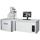
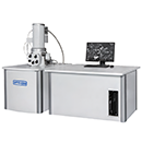
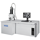
A63.7062 Eco Tungsten Filament SEM
|
| Resolution |
4.5nm@30KV(SE); 6nm@30KV(BSE) |
| Magnification |
Negative Magnification: 15x~250000x; Screen Magnification: 30x~500000x |
| Electron Gun |
Tungsten Heated Cathode-Pre Centered Tungsten Filament Cartridge |
| Accelerating Voltage |
0~30KV |
| Lens System |
Three-level Electromagnetic Lens (Tapered Lens) |
| Objective Aperture |
Molybdenum Aperture Adjustable Outside Vacuum System |
| Specimen Stage |
Five Axes Stage |
| Travel Range |
X(Auto) |
0~50mm |
| Y(Auto) |
0~50mm |
| Z(Manual) |
0~25mm |
| R(Manual) |
360o |
| T(Manual) |
-5o~90o |
| Max Specimen Diameter |
150mm |
| Detector |
High Vacuum Secondary Electron Detector (With Detector Protection) |
| Modification |
Stage Upgrade;EBL;STM;AFM;Heating Stage;Cryo Stage;Tensile Stage;Micro-nano Manipulator;SEM+Coating Machine;SEM+Laser |
| Accessories |
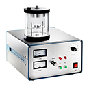
CCD,LaB6,X-Ray Detector(EDS),EBSD,CL,WDS,Coating Machine |
| Vacuum System |
Turbo Molecular Pumps;Rotation Pump |
| Electron Beam Current |
10pAt~0.1μA |
| PC |
Customized Dell Work Station |

 Biological Microscope
 Student Microscope